#Semiconductor Fabrication Material Market Share
Explore tagged Tumblr posts
Visit Tumblr Blog
Explore Tumblr blogs with no restrictions, modern design and the best experience.
Last Seen Tumblr Blogs


Fun Fact
In February 2021, Tumblr had 518.6 million blog accounts.
Text
Semiconductor Fabrication Material Market - Forecast(2024 - 2030)
Semiconductor Fabrication Material Market Overview
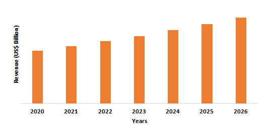
Semiconductor Fabrication Material Market size is forecast to reach US$84.5 billion by 2027 after growing at a CAGR of 6.3% during 2022-2027. Semiconductor fabrication refers to the process of manufacturing semiconductor products. It can be defined as the materials that are used to pattern semiconductor wafers. Materials such as silicon wafers, wet chemicals, industrial gases, chemical mechanical polishing (CMP) slurry and pads, photomasks, sputter targets, photoresists for semiconductors, photoresists for EUV, electrostatic chucks, IC lead frame, and others, are generally used as the semiconductor fabrication materials. One of the major factors driving the growth of the semiconductor fabrication material market is the increasing use of digitally integrated ICs in the electrical and electronics, automotive, and telecommunication industry. Also, the increasing growth of the semiconductor industry with rising advancements in the semiconductor solutions, is one of the primary reasons behind the upliftment of the semiconductor fabrication material market. For instance, as per the Semiconductor Industry Association (SIA) the global semiconductor industry sales in August 2021 registered US$47.2 billion, up 29.7% over August 2020's $36.4 billion total and 3.3 percent higher than July 2021's $45.7 billion total.
COVID-19 Impact
The COVID 19 outbreak has impacted the development of the semiconductor fabrication material market in 2020 owing to the lockdown measure in various region such as Asia-Pacific, North America and others. However, despite the Covid -19 pandemic, aerospace and defense contributed US$ 382 billion to the gross domestic product of the United States with US$ 90.6 billion from exports and has shown a growing trend as compared to 2019 with the export of US$ 40.6 billion, and revenue US$ 218.6 billion according to Aerospace and Defense Association.
Report Coverage
The report “Semiconductor Fabrication Material Market – Forecast (2022-2027)”, by IndustryARC, covers an in-depth analysis of the following segments of the semiconductor fabrication material market.
By Material Type: Wet Chemicals, Silicon Wafers, Industrial Gases, Chemical Mechanical Polishing (CMP) Slurry and Pads, Photomasks, Sputter Targets, Photoresists for Semiconductors, Photoresists for EUV, Electrostatic Chucks, IC Lead Frame, Wire Bonding, and Others
By Semiconductor Type: N-Type and P-Type
By Application: Consumer Appliances, Power Generation, Electronic Components, and Others
End Use Industry: Telecommunication, Energy, Electrical and Electronics, Medical and Healthcare, Automotive, Defence & Aerospace, and Others
By Geography: North America (USA, Canada and Mexico), Europe (UK, France, Germany, Italy, Spain, Russia, Netherlands, Belgium, and Rest of Europe), APAC (China, Japan, India, South Korea, Australia and New Zealand, Indonesia, Taiwan, Malaysia and Rest of APAC), South America (Brazil, Argentina, Colombia, Chile, Rest of South America), and Rest of the world (Middle East and Africa).
Request Sample
Key Takeaways
Asia-Pacific dominates the Semiconductor Fabrication Material Market owing to rapid increase in electrical and electronic sector.
N-Type are the most commonly used semiconductor type which is used to obtain a majority charge carrier of free electrons making them more conductive than intrinsic semiconductors.
The rise in demand from various end-use industries like telecommunication, consumer appliances, and others are expected to boost the demand for the semiconductor fabrication material market during the forecast period.
High cost for raw material is the major restrain for the market growth.
Semiconductor Fabrication Material Market Segment Analysis - By Semiconductor Type
N-type segment held the largest share in the semiconductor fabrication material market in 2021 and is estimated to rise at a CAGR of 6.8% in terms of revenue during the forecast period from 2022-2027. N-type semiconductors are key materials in the formation of p-n junctions, where a p-type and an n-type semiconductor are brought in close contact to create a depletion region. Holes and electrons recombine in this region and result in the production of light, thus obtaining Light Emitting Diodes (LED’s). According to the U.S. Department of Energy, China dominates the LED manufacturing market. In 2019, the total size of the North American LED luminaire market was estimated to be US$ 11.6 billion of which the United States was about US$ 8.14 billion. The growing LED industry as well as the Electronics Industry and new developments like the launch of new products, expansions, and acquisitions, are the key factors contributing to the growth of this segment.
Inquiry Before Buying
Semiconductor Fabrication Material Market Segment Analysis - By End-Use Industry
Electrical and electronics sector held the largest share in the semiconductor fabrication material market in 2021 and is estimated to rise at a CAGR of 7.8%% in terms of revenue during the forecast period from 2022-2027. The Semiconductors fabrication materials are used in the manufacture of different kinds of electronic devices, including diodes, transistors, chips control temperatures, timers, automated features and integrated circuits. Electrical and electronic appliances make life easier with smart technology and the internet of things is an advantage. As a result, semiconductor chips help to work with multi-functionality feature to respond to rising demand & maintain standards, and highly durable services. According to IPC Economic outlook December 2021, the electronics industry, which includes categories such as components, loaded boards, computers, communications equipment, and consumer electronics is being increased by 2.6% in November 2021. The electrical and electronic sector sales have been increased by 30.6% as compared to 2019 and 12.8% in 2019-2021. Therefore, the growing electronic manufacturing will increase the demand for semiconductor fabrication material during the forecast period.
Semiconductor Fabrication Material Market Segment Analysis - By Geography
Asia-Pacific region held the largest share in the semiconductor fabrication material market and growing at CAGR of 7.9% during 2022-2027. China’s semiconductor sector has expanded to become one of the largest in the world and also is the biggest consumer of chips. For instance, according to the Semiconductor Industry Association (SIA), the Chinese semiconductor industry is estimated to invest US$12.3 billion in 2021 and US$15.3 billion in 2022, on CAPEX contributing about 15% of the global total. On the other hand, the increasing investments in the semiconductor industry, with the rising installation of new plants will drive the market growth of Japan’s semiconductor fabrication material. For instance, the Japanese government invested US$6.8 billion for domestic production of semiconductors to make the nation a major global provider of essential computer chips. Furthermore, India’s semiconductor sector has expanded with the increasing government investment and rise in the end use industries such as energy and telecommunication, is driving the market growth of semiconductor fabrication material market over the forecast period. For instance, according to the India Briefing, in 2021 the government funded US$10 billion to boost semiconductor and display manufacturing in the country, in order to attract large chip makers and make India as hi-tech production hub globally.
Schedule a Call
Semiconductor Fabrication Material Market Drivers
Rise in demand from End use Industry
Increased use of semiconductors in various end-use industries such as telecommunication, consumer appliances, and others are expected to boost the demand for the semiconductor fabrication material market during the forecast period. The modern period of telecommunication commenced with the use of semiconductor devices in telecommunication technology. The transistors technology helped develop existing technology from narrow broadband to private packet-switched networks. 5G network is another technology achieved with the help of semiconductor technology and can transfer large amounts of data 100-200X faster than 4G LTE. However, various components of the internet of things infrastructures like processors, modems, and logic chips helped increase memory output and performance. Therefore, the use of semiconductor devices in telecommunication is boosting the demand for semiconductor fabrication material during the forecast period. Power semiconductors consist of power sensors, SiC devices, power control integrated circuits, rectifier diodes. These devices are widely used in consumer appliances produced by semiconductor fabrication materials like chips, logic, wafer, memory, etc. According to the Association of Home Manufacturer appliances, the home appliances industry has generated US$198.14 billion throughout the U.S. economy and CAD 5.8 billion in output across Canada in 2020.
Increasing Government Initiative for new semiconductor production units
The government initiation plays a vital role in the development of any sector. The investment by the government helps to boost the demand and market share. The U.S. government has taken the initiation to fortify America's semiconductor supply chains through robust investments in U.S. chip production and innovation. In June 2021, the U.S government passed the fund to United States Innovation and Competition Act (USICA), broad competitiveness legislation that includes US$ 52 billion to bolster domestic chip manufacturing, research, and design. The semiconductor industry has urged the U.S. House of Representatives to follow suit and send legislation to the President's desk to be signed into law. In addition, leading Chinese foundries and several foundry start-ups have accelerated their pace of building trailing-edge fabs. According to VLSI, China’s memory and foundry capacity is expected to grow at a CAGR of 14.7% over the next 10 years. In 2020- 2021, semiconductors helped world to move steadily to overcome the hurdles faced by COVID-19. As semiconductor innovation and global chip demand continue their inextricable rise, government and industry must work together for the production of semiconductor. Therefore, the growing total cost of ownership will help in the development of semiconductor in the country and helping to increase the demand for semiconductor fabrication material during the forecast period.
Buy Now
Semiconductor Fabrication Material Market Challenges
High Cost for Raw Material
In the recent time there has been an increase in the prices of raw materials that are used for Semiconductor fabrication material manufacturing such as silicon chips, wafers, industrial gases, and others owing to which there is an increase in the price of Semiconductor Fabrication Material as well. A silicone is made from the second-most abundant element on Earth which has become scarce, is increasing concern to car parts to computer chips. The shortage in silicon metal had cut the production in China, and prices has grown up in between May 2021 – October 2021. Also, the costs of semiconductor are proportional to its function and performance in order to meet building code requirements. Semiconductors undergoes extensive research and testing to ensure that quality and performance standards are met, and as a result, it is more highly priced. Therefore, all the above factors significantly contribute towards the high cost of semiconductors, thereby posing as a significant challenge for the semiconductor fabrication material market during the forecast period.
Semiconductor Fabrication Material Market Landscape
Technology launches, acquisitions and R&D activities are key strategies adopted by players in the semiconductor fabrication material. Major players in the semiconductor fabrication material market are:
DuPont de Nemours, Inc.,
Shin-Etsu Chemical Co. Ltd.
Sumco Corporation
Air Liquide S.A
JSR Corporation
Versum Materials Inc.
Globalwafers
Sumitomo Chemical,
Photronics, Inc.
Honeywell International Inc.
Recent Developments
In April 2021, CMC Materials acquired International Test Solutions which will enable them to help solve their customers’ most demanding challenges and maximize their yield & throughput in the semiconductor manufacturing process.
In November 2020, Showa Denko Materials, Co., Ltd., in collaboration with Chengdu Kemeite Special Gas Co., Ltd., established a new subsidiary, Chengdu Kemeite Showa Electronic Materials Co., Ltd., which aims to strengthen SDK’s business to produce and sell high-purity gases for electronics.
#Semiconductor Fabrication Material Market#Semiconductor Fabrication Material Market Share#Semiconductor Fabrication Material Market Size#Semiconductor Fabrication Material Market Forecast#Semiconductor Fabrication Material Market Report#Semiconductor Fabrication Material Market Growth
0 notes
Text

#Semiconductor Fabrication Materials Market#Semiconductor Fabrication Materials Market Size#Semiconductor Fabrication Materials Market Share#Semiconductor Fabrication Materials Market Trends
0 notes
Text
Quartz Glass for Photovoltaic and Semiconductor Market, Global Outlook and Forecast 2025-2032
Quartz glass, also known as fused silica, is a high-performance material that is widely used across various industries, especially in photovoltaics and semiconductors. Quartz glass products for these industries include items such as quartz boats, furnace tubes, flanges, and other specialized instruments. This material stands out for its unique properties, including high-temperature resistance, optical clarity, and excellent mechanical strength, making it indispensable in applications where precision and durability are paramount.
In the semiconductor industry, quartz glass is essential due to its ability to withstand the extreme conditions involved in the manufacturing process, such as high temperatures and aggressive chemical environments. For photovoltaics, quartz glass products are used in the production of solar cells and panels, where they serve to improve the efficiency of solar energy conversion while ensuring stability over time.
In essence, the market for quartz glass for photovoltaic and semiconductor applications revolves around a demand for high-quality, durable, and thermally stable materials that can withstand the complexities of semiconductor fabrication and the energy demands of the solar industry.
Download a Free Report PDF @ https://www.24chemicalresearch.com/download-sample/286846/global-quartz-glass-for-photovoltaic-semiconductor-forecast-market-2025-2032-180
Market Size
The global market for Quartz Glass in Photovoltaic and Semiconductor applications was valued at approximately USD 238.20 million in 2023. The industry is projected to grow at a compound annual growth rate (CAGR) of 16.50% during the forecast period, with a market size expected to reach USD 693.78 million by 2032.
This significant growth is primarily driven by the increasing demand for energy-efficient technologies, particularly in the semiconductor and photovoltaic sectors. The ongoing advancements in semiconductor fabrication processes and the expansion of solar energy installations are key factors contributing to the expansion of the quartz glass market.
North America holds a substantial share of the market, with the North American Quartz Glass for Photovoltaic and Semiconductor market valued at USD 62.07 million in 2023. The region is expected to witness a CAGR of 14.14% during the period from 2025 through 2032, driven by the rising adoption of renewable energy and advancements in semiconductor technology.
Market Dynamics (Drivers, Restraints, Opportunities, and Challenges)
Drivers
Increasing Demand for Solar Energy: As the world moves toward cleaner energy, the photovoltaic industry is booming. Quartz glass products, such as furnace tubes and quartz boats, are essential for producing high-efficiency solar panels, driving demand for these materials.
Technological Advancements in Semiconductors: The semiconductor industry’s continuous innovation in chip fabrication technology requires high-performance materials like quartz glass, known for its ability to handle extreme conditions during the manufacturing process.
Energy Efficiency Initiatives: Global efforts to reduce energy consumption and increase energy efficiency across industries are propelling the growth of technologies that rely on quartz glass, such as solar power systems and semiconductor devices.
Durability and Reliability: Quartz glass’s inherent resistance to thermal and chemical stresses makes it indispensable for applications in environments that demand precision and durability, which drives its widespread adoption.
Restraints
High Manufacturing Costs: The cost of producing high-quality quartz glass is significant due to the raw material costs, energy consumption, and intricate production processes. This can make it difficult for smaller companies to enter the market or for manufacturers to reduce costs.
Limited Availability of Raw Materials: Quartz is not an easily accessible material in all regions. The supply of high-quality quartz, especially for high-tech applications, can be constrained by geographic and environmental factors.
Competition from Alternative Materials: While quartz glass has distinct advantages, there is growing competition from alternative materials like ceramics and other glass variants, which could limit its market share, especially in cost-sensitive applications.
Opportunities
Expansion of Renewable Energy Projects: With increasing global investments in solar energy, there is a significant opportunity for the quartz glass market to grow. Solar panel production requires high-purity quartz glass, and as photovoltaic installations increase, so too does the demand for this material.
Growth in Semiconductor Technology: As industries such as electronics, automotive, and healthcare continue to require smaller, more powerful semiconductors, the demand for quartz glass products used in semiconductor manufacturing is likely to see a boost.
Innovations in Quartz Glass Manufacturing: Advances in manufacturing techniques and recycling processes for quartz glass could lower production costs and make the material more accessible to emerging markets, expanding its use across more industries.
Challenges
Environmental Impact of Production: The production of quartz glass involves high energy consumption, which can have significant environmental implications. As sustainability becomes a critical issue, manufacturers will face pressure to reduce their carbon footprint.
Supply Chain Disruptions: The quartz glass market is dependent on global supply chains for both raw materials and finished products. Any disruption—such as geopolitical tensions, trade restrictions, or natural disasters—can affect the availability and pricing of quartz glass.
Regional Analysis
The global quartz glass market for photovoltaic and semiconductor applications is witnessing diverse trends across regions:
North America: With a rapidly growing renewable energy sector and a robust semiconductor manufacturing base, North America holds a significant share of the market. The U.S. is a leader in solar energy adoption and semiconductor innovation, contributing to the region's growth in demand for high-quality quartz glass products.
Asia-Pacific: Asia-Pacific, particularly China, Japan, and South Korea, is expected to dominate the market due to the massive scale of semiconductor manufacturing and solar energy projects. These countries are home to leading semiconductor manufacturers and solar panel producers, making them key drivers of the quartz glass market in the region.
Europe: Europe is increasingly focused on renewable energy sources, and countries like Germany and France are major players in the photovoltaic industry. The region’s push for sustainability and energy efficiency is expected to drive the demand for quartz glass products.
Latin America: While the demand in Latin America is growing, it is still in the early stages compared to North America and Asia-Pacific. However, with increasing investments in renewable energy projects, the region presents promising opportunities for the quartz glass market.
Middle East and Africa: The Middle East has a large solar energy potential, particularly in countries like Saudi Arabia and the UAE. The demand for quartz glass in this region is expected to rise as solar energy infrastructure develops.
Competitor Analysis
The quartz glass market for photovoltaics and semiconductors is competitive, with several key players dominating the industry:
Heraeus: A leading global provider of high-performance materials, Heraeus offers a wide range of quartz glass products for semiconductor and photovoltaic applications.
Tosoh Quartz Corporation: Known for its high-purity quartz products, Tosoh Quartz plays a significant role in the semiconductor market.
Shin-Etsu: One of the world’s largest semiconductor material suppliers, Shin-Etsu provides advanced quartz glass solutions used in semiconductor manufacturing processes.
Schunk: This company manufactures quartz glass products for a wide range of industries, including photovoltaics and semiconductors.
MARUWA: A key player in the Japanese market, MARUWA produces quartz glass products for use in semiconductor production.
These companies are consistently innovating in product design and manufacturing processes to meet the growing demands of the photovoltaic and semiconductor industries.
Global Quartz Glass for Photovoltaic and Semiconductor: Market Segmentation Analysis
This report provides a deep insight into the global Quartz Glass for Photovoltaic and Semiconductor market, covering all its essential aspects. This ranges from a macro overview of the market to micro details of the market size, competitive landscape, development trend, niche market, key market drivers and challenges, SWOT analysis, value chain analysis, etc.
The analysis helps the reader to shape the competition within the industries and strategies for the competitive environment to enhance the potential profit. Furthermore, it provides a simple framework for evaluating and assessing the position of the business organization. The report structure also focuses on the competitive landscape of the Global Quartz Glass for Photovoltaic and Semiconductor Market. This report introduces in detail the market share, market performance, product situation, operation situation, etc., of the main players, which helps the readers in the industry to identify the main competitors and deeply understand the competition pattern of the market.
In a word, this report is a must-read for industry players, investors, researchers, consultants, business strategists, and all those who have any kind of stake or are planning to foray into the Quartz Glass for Photovoltaic and Semiconductor market in any manner.
Market Segmentation (by Application)
Photovoltaic
Semiconductor
Market Segmentation (by Type)
High Temperature Process
Low Temperature Process
Key Company
Heraeus
Tosoh Quartz Corporation
Shin-Etsu
Schunk
MARUWA
Shenyang Hanke
Phillipa Stone
Beijing Cade Quartz
Shanghai Qianghua Industry
Hangzhou Daiwa Thermal Magnetic Electronics Co. Ltd.
Hangzhou Tegno
Ningbo Yunde Semiconductor
Dongke Quartz
Hongxin Semiconductor
Jiangsu Hongyang Quartz Products
Jiangsu Hongwei Quartz Technology
Zhejiang Aobo Quartz Technology
Jiangsu Xinyiding Quartz Technology
Topband Hongji
Geographic Segmentation
North America (USA, Canada, Mexico)
Europe (Germany, UK, France, Russia, Italy, Rest of Europe)
Asia-Pacific (China, Japan, South Korea, India, Southeast Asia, Rest of Asia-Pacific)
South America (Brazil, Argentina, Columbia, Rest of South America)
The Middle East and Africa (Saudi Arabia, UAE, Egypt, Nigeria, South Africa, Rest of MEA)
FAQ
What is the current market size of Quartz Glass for Photovoltaic and Semiconductor?
➣ The market size of Quartz Glass for Photovoltaic and Semiconductor was estimated at USD 238.20 million in 2023 and is projected to reach USD 693.78 million by 2032.
Which are the key companies operating in the Quartz Glass for Photovoltaic and Semiconductor market?
➣ Key players include Heraeus, Tosoh Quartz Corporation, Shin-Etsu, Schunk, and MARUWA.
What are the key growth drivers in the Quartz Glass for Photovoltaic and Semiconductor market?
➣ The key growth drivers are the increasing demand for renewable energy, advancements in semiconductor technology, and the growing focus on energy efficiency.
Which regions dominate the Quartz Glass for Photovoltaic and Semiconductor market?
➣ Asia-Pacific, North America, and Europe are dominant in the market, driven by semiconductor manufacturing and solar energy adoption.
What are the emerging trends in the Quartz Glass for Photovoltaic and Semiconductor market?
➣ Emerging trends include innovations in quartz glass manufacturing techniques, the growth of renewable energy, and increasing investments in semiconductor production technologies. Key Benefits of This Market Research:
Industry drivers, restraints, and opportunities covered in the study
Neutral perspective on the market performance
Recent industry trends and developments
Competitive landscape & strategies of key players
Potential & niche segments and regions exhibiting promising growth covered
Historical, current, and projected market size, in terms of value
In-depth analysis of the Quartz Glass for Photovoltaic and Semiconductor Market
Overview of the regional outlook of the Quartz Glass for Photovoltaic and Semiconductor Market:
Key Reasons to Buy this Report:
Access to date statistics compiled by our researchers. These provide you with historical and forecast data, which is analyzed to tell you why your market is set to change
This enables you to anticipate market changes to remain ahead of your competitors
You will be able to copy data from the Excel spreadsheet straight into your marketing plans, business presentations, or other strategic documents
The concise analysis, clear graph, and table format will enable you to pinpoint the information you require quickly
Provision of market value (USD Billion) data for each segment and sub-segment
Indicates the region and segment that is expected to witness the fastest growth as well as to dominate the market
Analysis by geography highlighting the consumption of the product/service in the region as well as indicating the factors that are affecting the market within each region
Competitive landscape which incorporates the market ranking of the major players, along with new service/product launches, partnerships, business expansions, and acquisitions in the past five years of companies profiled
Extensive company profiles comprising of company overview, company insights, product benchmarking, and SWOT analysis for the major market players
The current as well as the future market outlook of the industry concerning recent developments which involve growth opportunities and drivers as well as challenges and restraints of both emerging as well as developed regions
Includes in-depth analysis of the market from various perspectives through Porter’s five forces analysis
Provides insight into the market through Value Chain
Market dynamics scenario, along with growth opportunities of the market in the years to come
6-month post-sales analyst support
Download a Free Report PDF @ https://www.24chemicalresearch.com/download-sample/286846/global-quartz-glass-for-photovoltaic-semiconductor-forecast-market-2025-2032-180
0 notes
Text
Semiconductor Abatement Systems Market Report 2024-2032 by Reports and Insights

The Reports and Insights, a leading market research company, has recently releases report titled “Semiconductor Abatement Systems Market: Global Industry Trends, Share, Size, Growth, Opportunity and Forecast 2024-2032.” The study provides a detailed analysis of the industry, including the global Semiconductor Abatement Systems Market share, size, trends, and growth forecasts. The report also includes competitor and regional analysis and highlights the latest advancements in the market.
Report Highlights:
How big is the Semiconductor Abatement Systems Market?
The global semiconductor abatement systems market size reached US$ 800.7 million in 2023. Looking forward, Reports and Insights expects the market to reach US$ 1,998.9 million in 2032, exhibiting a growth rate (CAGR) of 10.7% during 2024-2032.
What are Semiconductor Abatement Systems?
Semiconductor abatement systems are advanced tools used in the semiconductor manufacturing process to remove hazardous gases and chemicals. These systems play a critical role in maintaining a safe and clean working environment by efficiently neutralizing and treating exhaust gases and process by-products. Semiconductor abatement systems are essential for controlling emissions and ensuring compliance with environmental regulations in semiconductor fabrication facilities. They are designed to handle a wide range of toxic gases, including fluorine, chlorine, and arsine, providing a reliable and efficient solution for managing waste gases in semiconductor manufacturing.
Request for a sample copy with detail analysis: https://www.reportsandinsights.com/sample-request/1856
What are the growth prospects and trends in the Semiconductor Abatement Systems industry?
The semiconductor abatement systems market growth is driven by various and trends. The market for semiconductor abatement systems is a critical component of the semiconductor industry, fueled by the rising need for advanced manufacturing processes and strict environmental guidelines. These systems play a vital role in eliminating hazardous gases and chemicals used in semiconductor manufacturing, ensuring both a safe workplace and adherence to regulatory standards. Market growth is driven by factors like increased adoption of abatement systems in semiconductor fabrication plants, a growing emphasis on sustainability, and the demand for effective solutions for managing waste gases. Furthermore, ongoing technological advancements, including the creation of more efficient and economical abatement systems, are driving the market's expansion. Hence, all these factors contribute to semiconductor abatement systems market growth.
What is included in market segmentation?
The report has segmented the market into the following categories:
By Type:
Wet Abatement Systems
Dry Abatement Systems
By Process:
Etch Abatement Systems
Chemical Vapor Deposition (CVD) Abatement Systems
Physical Vapor Deposition (PVD) Abatement Systems
Chemical Mechanical Planarization (CMP) Abatement Systems
Others
By End-Use:
Semiconductor Manufacturers
Foundries
Packaging and Assembly Service Providers
Others
By Application:
Logic and Memory Devices
Micro-electromechanical Systems (MEMS)
Power Devices
Optoelectronics
Others
By Sales Channel:
Direct Sales
Distributor Sales
Market Segmentation By Region:
North America
United States
Canada
Europe
Germany
United Kingdom
France
Italy
Spain
Rest of Europe
Asia Pacific
China
Japan
India
South Korea
Rest of Asia Pacific
Latin America
Brazil
Mexico
Argentina
Middle East & Africa
Saudi Arabia
South Africa
United Arab Emirates
Israel
Who are the key players operating in the industry?
The report covers the major market players including:
Applied Materials Inc.
Lam Research Corporation
Tokyo Electron Limited
Hitachi High-Technologies Corporation
Axcelis Technologies Inc.
Edwards Vacuum LLC
Aeronex Inc.
DAS Environmental Expert GmbH
MKS Instruments Inc.
AMEC International Limited
TEL NEXX, Inc.
Ultra Clean Holdings, Inc.
CVD Equipment Corporation
View Full Report: https://www.reportsandinsights.com/report/Semiconductor Abatement Systems-market
If you require any specific information that is not covered currently within the scope of the report, we will provide the same as a part of the customization.
About Us:
Reports and Insights consistently mееt international benchmarks in the market research industry and maintain a kееn focus on providing only the highest quality of reports and analysis outlooks across markets, industries, domains, sectors, and verticals. We have bееn catering to varying market nееds and do not compromise on quality and research efforts in our objective to deliver only the very best to our clients globally.
Our offerings include comprehensive market intelligence in the form of research reports, production cost reports, feasibility studies, and consulting services. Our team, which includes experienced researchers and analysts from various industries, is dedicated to providing high-quality data and insights to our clientele, ranging from small and medium businesses to Fortune 1000 corporations.
Contact Us:
Reports and Insights Business Research Pvt. Ltd. 1820 Avenue M, Brooklyn, NY, 11230, United States Contact No: +1-(347)-748-1518 Email: [email protected] Website: https://www.reportsandinsights.com/ Follow us on LinkedIn: https://www.linkedin.com/company/report-and-insights/ Follow us on twitter: https://twitter.com/ReportsandInsi1
#Semiconductor Abatement Systems Market share#Semiconductor Abatement Systems Market size#Semiconductor Abatement Systems Market trends
0 notes
Text
2D Material Semiconductors: A $7.5B Industry by 2034!
2D material semiconductors market is poised for significant expansion, with its valuation expected to grow from $1.8 billion in 2024 to $7.5 billion by 2034, reflecting a robust compound annual growth rate (CAGR) of approximately 15.2%. This market encompasses the development, production, and commercialization of two-dimensional semiconductor materials, which are characterized by their atomic-scale thickness and exceptional electronic properties. Key materials in this market include graphene, transition metal dichalcogenides (TMDs), and other novel substances that are driving advancements in electronics, optoelectronics, and flexible devices. These materials support innovation in next-generation transistors, sensors, and energy-efficient technologies, offering transformative potential across sectors such as telecommunications, computing, and renewable energy.
To Request Sample Report: https://www.globalinsightservices.com/request-sample/?id=GIS10001 &utm_source=SnehaPatil&utm_medium=Article
The 2D material semiconductors market is experiencing robust growth, primarily fueled by advancements in electronics and optoelectronics. Graphene leads the market segment due to its superior electrical conductivity and mechanical strength. Transition metal dichalcogenides (TMDs) represent the second-largest segment, owing to their unique electronic properties and versatility in various applications. The increasing demand for high-performance, energy-efficient devices in the consumer electronics sector serves as a major market driver. North America dominates the market, benefiting from significant investments in research and development and a strong technological infrastructure. Meanwhile, Asia-Pacific follows closely, driven by rapid industrialization, a burgeoning electronics industry, and substantial government support for semiconductor innovation. Countries such as the United States and China are leading the adoption of 2D materials in advanced technologies. The market’s growth is further supported by ongoing collaborations between academia and industry, which aim to explore new applications and enhance material performance.
Buy Now : https://www.globalinsightservices.com/checkout/single_user/GIS10001/?utm_source=SnehaPatil&utm_medium=Article
Market segmentation for the 2D material semiconductors industry covers various aspects. In terms of type, key categories include graphene, transition metal dichalcogenides (TMDs), black phosphorus, and hexagonal boron nitride. The product segment comprises transistors, photodetectors, sensors, and memory devices. Various technologies such as chemical vapor deposition (CVD), mechanical exfoliation, liquid phase exfoliation, and molecular beam epitaxy (MBE) are employed in production. Applications span across diverse sectors, including consumer electronics, automotive, aerospace and defense, healthcare, energy storage, and optoelectronics. Furthermore, material types are classified into monolayer, bilayer, and few-layer structures, while devices include field-effect transistors (FETs), light-emitting diodes (LEDs), and photovoltaic cells. The market also accounts for processes such as synthesis, integration, fabrication, and characterization, serving end users like semiconductor manufacturers, research institutes, consumer electronics companies, and automotive manufacturers.
In 2023, the 2D material semiconductors market was estimated to have a volume of 350 million units, with projections to reach 600 million units by 2033. The graphene segment currently dominates the market with a 45% share, followed by transition metal dichalcogenides at 30% and phosphorene at 25%. Graphene’s dominance is driven by its superior electrical properties and widespread application across industries, including electronics and energy storage. Major players in the market include companies such as Graphenea, 2D Semiconductors, and AMO GmbH, which hold significant market shares and play a pivotal role in advancing material innovation and application.
The competitive landscape is shaped by strategic alliances and R&D investments aimed at enhancing material properties and expanding application areas. Regulatory frameworks, particularly in regions such as the EU and the US, are increasingly focusing on safety and environmental impacts, influencing market dynamics. Future projections indicate an annual growth rate of 15%, driven by technological advancements and increased adoption in flexible electronics and optoelectronics. Despite challenges such as high production costs and scalability issues, the integration of AI in material design and manufacturing processes is anticipated to mitigate these hurdles and unlock new opportunities for market expansion.
#2DMaterials #SemiconductorInnovation #GrapheneTechnology #FlexibleElectronics #Optoelectronics #TMDs #NextGenTransistors #EnergyEfficientDevices #TechAdvancements #ConsumerElectronics #FutureOfSemiconductors #R&DInvestments #EmergingTechnologies #SmartDevices #MaterialScience
0 notes
Text
🌍 "The Dual Face of Carbon Monoxide: Market Analysis & Insights"
Carbon Monoxide (CO) Market plays a crucial role in diverse industries, serving as a critical feedstock and reducing agent. From chemical manufacturing and metallurgy to electronics and pharmaceuticals, CO is vital for optimizing processes and enhancing product quality.
To Request Sample Report : https://www.globalinsightservices.com/request-sample/?id=GIS21633 &utm_source=SnehaPatil&utm_medium=Article
Market Insights 🌟
Chemical Manufacturing leads the market with 45% share, driven by CO’s applications in chemical synthesis and metal fabrication.
The automotive sector follows with 30% share, where CO is used in exhaust systems.
The electronics industry holds 25% share, leveraging CO in semiconductor manufacturing for chemical vapor deposition.
In 2023, the market volume reached 250 million metric tons, projected to grow to 400 million metric tons by 2033.
Regional Highlights 🌐
North America dominates the market, with the United States leading due to stringent safety standards and robust industrial infrastructure.
Europe ranks second, with countries like Germany benefiting from strong automotive and chemical sectors. The European Union’s emphasis on reducing emissions also boosts CO demand.
Asia-Pacific shows promising growth, driven by industrial expansion in countries like China and India.
Future Outlook 🔮
Technological advancements and increased R&D investments (expected to grow by 15% by 2033) are driving sustainable production methods and improving the efficiency of CO applications. While challenges like fluctuating raw material costs and regulatory compliance persist, emerging opportunities in carbon capture technologies and sustainable manufacturing hold immense potential.
Top Players 🏢
Major players like Linde plc, Air Liquide, and Praxair lead the market through advanced production technologies and strategic partnerships.:
#CarbonMonoxideMarket #IndustrialInnovation #CleanProduction #ChemicalManufacturing #MetallurgyTech #ElectronicsIndustry #AutomotiveInnovation #SustainableGrowth #CarbonCapture #GasCylinders #SemiconductorTech #IndustrialSolutions #COApplications #GreenManufacturing #MarketGrowth
0 notes
Text
The Chemical Mechanical Planarization Market is projected to grow from USD 5402.5 million in 2024 to an estimated USD 8291.14 million by 2032, with a compound annual growth rate (CAGR) of 5.5% from 2024 to 2032.The Chemical Mechanical Planarization (CMP) market has emerged as a critical segment within the semiconductor and electronics industry, driving innovation and growth through its pivotal role in manufacturing processes. CMP is an essential technique employed in semiconductor fabrication to achieve flat and smooth wafer surfaces, which are crucial for high-performance integrated circuits. As technological advancements accelerate and consumer demand for sophisticated electronic devices grows, the CMP market is poised for significant expansion.
Browse the full report at https://www.credenceresearch.com/report/chemical-mechanical-planarization-market
Market Size and Growth Projections
The global CMP market is projected to experience robust growth, with its valuation estimated to increase from USD 5.2 billion in 2024 to approximately USD 8.7 billion by 2032. This represents a compound annual growth rate (CAGR) of 6.8% during the forecast period. This growth is fueled by escalating demand for advanced semiconductor devices across industries such as telecommunications, consumer electronics, automotive, and healthcare. The proliferation of technologies like 5G, artificial intelligence (AI), and the Internet of Things (IoT) further amplifies the need for efficient and reliable planarization processes, thereby bolstering the CMP market.
Key Market Drivers
Rising Demand for Miniaturization
As devices become more compact and powerful, the semiconductor industry is increasingly adopting smaller node technologies. CMP plays a crucial role in achieving the required precision and uniformity in these advanced nodes. The demand for miniaturization in consumer electronics, smartphones, and wearables drives the adoption of CMP processes.
Growth in 5G and IoT Applications
The deployment of 5G networks and the widespread adoption of IoT applications necessitate the development of high-performance semiconductors. CMP is indispensable in fabricating these chips, ensuring optimal performance and reliability. The expanding ecosystem of connected devices further strengthens the CMP market’s prospects.
Advancements in CMP Materials and Equipment
The development of innovative CMP slurries, pads, and equipment is enhancing the efficiency and effectiveness of planarization processes. These advancements address challenges such as defect reduction, process optimization, and cost efficiency, making CMP more attractive to semiconductor manufacturers.
Growth in Automotive Electronics
The automotive sector’s increasing reliance on electronic components, including advanced driver-assistance systems (ADAS), electric vehicle (EV) systems, and infotainment systems, is driving the demand for high-quality semiconductors. CMP ensures the production of defect-free wafers, aligning with the automotive industry’s stringent quality standards.
Challenges and Opportunities
Despite its growth prospects, the CMP market faces challenges such as high equipment costs, complexity in process integration, and stringent environmental regulations. However, these challenges present opportunities for innovation. The development of eco-friendly CMP solutions, advancements in process automation, and the integration of artificial intelligence and machine learning for process optimization are areas ripe for exploration.
Key Players and Competitive Landscape
The CMP market is characterized by the presence of established players and emerging innovators. Key companies include Applied Materials, Inc., Lam Research Corporation, Ebara Corporation, DuPont, Entegris, Inc., and Cabot Microelectronics. These players are investing heavily in R&D to enhance their product offerings and maintain a competitive edge. Strategic partnerships, mergers, and acquisitions are also prevalent as companies aim to expand their market presence and technological capabilities.
Future Outlook
The Chemical Mechanical Planarization market is poised for sustained growth, driven by technological advancements, rising demand for high-performance semiconductors, and the proliferation of next-generation applications. As the semiconductor industry continues to evolve, the CMP market will remain integral to achieving the precision and efficiency required for cutting-edge technologies. With ongoing innovation and strategic investments, the market holds promising prospects for stakeholders across the value chain.
Key Player Analysis:
Air Products and Chemicals, Inc.
Applied Materials Inc.
Cabot Microelectronics Corporation
CMC Materials
DOW Electronic Materials
Ebara Corporation
Fujimi Incorporation
Hitachi Chemical Company, Ltd.
LAM Research Corporation
Lapmaster Wolters GmbH
Okamoto Machine Tool Works, Ltd.
Segmentation:
By Type:
CMP Consumable
CMP Equipment
By Technology:
Leading Edge
More than Moore’s
Emerging
By Application:
Integrated Circuits
MEMS and NEMS
Compound Semiconductors
Optics
By Region:
North America
U.S.
Canada
Mexico
Europe
Germany
France
U.K.
Italy
Spain
Rest of Europe
Asia Pacific
China
Japan
India
South Korea
South-east Asia
Rest of Asia Pacific
Latin America
Brazil
Argentina
Rest of Latin America
Middle East & Africa
GCC Countries
South Africa
Rest of the Middle East and Africa
Browse the full report at https://www.credenceresearch.com/report/chemical-mechanical-planarization-market
Contact:
Credence Research
Please contact us at +91 6232 49 3207
Email: [email protected]
0 notes
Text
High purity Alumina Market
High Purity Alumina Market Size, Share, Trends: Sumitomo Chemical Co., Ltd. Leads
Surging Demand for HPA in Li-Ion Battery Separators Boosts Market Growth
Market Overview:
The High Purity Alumina (HPA) market is expected to develop at a CAGR of 21.8% between 2024 and 2031. The market value is predicted to rise from XX USD in 2024 to YY USD in 2031. Asia-Pacific is expected to be the leading region in this market. Key metrics include rising demand for LED manufacture, increased utilisation in lithium-ion batteries, and expanding applications in semiconductor substrates. The HPA market is increasing rapidly, owing to the expanding electronics sector and the shift towards energy-efficient lighting options. The growing use of HPA in smartphones, electric vehicles, and renewable energy storage systems is driving market growth. Furthermore, the material's distinctive features, such as high thermal conductivity and superior electrical insulation, are propelling its employment in a variety of high-tech applications.
DOWNLOAD FREE SAMPLE
Market Trends:
The high purity alumina industry is seeing a considerable increase in the use of HPA as a coating material for lithium-ion battery separators. The rising electric vehicle (EV) sector and the developing portable electronics industry are driving this application forward. Stringent safety rules in the automobile sector, as well as the demand for longer-lasting, more efficient batteries in consumer electronics, have fuelled this trend. Major battery manufacturers are including HPA-coated separators into their designs, creating a rise in demand. This tendency is projected to continue as the EV market expands, with forecasts predicting that EVs will account for up to 30% of worldwide car sales by 2030.
Market Segmentation:
The 4N (99.99% purity) segment dominates the High Purity Alumina market, owing to its widespread application in the fabrication of LED sapphire substrates and semiconductor wafers. This purity grade provides the best blend of performance and cost-effectiveness, making it the preferred option for many high-tech applications. According to the global study, the LED market will be worth $YY billion by 2024, rising at a CAGR of 12.5% between 2024 and 2031. The worldwide semiconductor market is expected to approach $600 billion by 2025, creating significant opportunities for 4N HPA vendors.
Market Key Players:
The HPA market is highly competitive, with major players focusing on technological innovation and strategic alliances. Key companies such as Sumitomo Chemical Co., Ltd., Sasol Limited, Baikowski SAS, Nippon Light Metal Holdings Company, Ltd., Altech Chemicals Limited, Polar Sapphire Ltd., Hebei Heng Bo New Material Technology Co., Ltd., Zibo Honghe Chemical Co., Ltd., Xuan Cheng Jing Rui New Material Co., Ltd., and Orbite Technologies Inc. dominate the market.
Contact Us:
Name: Hari Krishna
Email us: [email protected]
Website: https://aurorawaveintellects.com/
0 notes
Text
Electroactive Polymers Market — By Type , By Application , By Geography — Global Opportunity Analysis & Industry Forecast, 2024–2030
Electroactive Polymers Market Overview

Request Sample :
Electroactive Polymers Market COVID-19 Pandemic
The outbreak of Covid-19 is having a huge impact on the economy of electronic devices. The COVID-19 pandemic caused an unprecedented increased demand for some medical devices, as well as significant disruptions in the manufacturing and supply chain operations of global medical devices. The FDA monitors the supply chain of medical products and works closely with producers and other stakeholders to assess the risk of disruption and to prevent or reduce its impact on patients, health care providers, and the general public’s health. In addition, there is a delay in imports and exports of medical devices due to the import-export restriction by the governments in various regions. All these factors are having a major impact on the Electroactive Polymers Market during the pandemic.
Report Coverage
The report: “Electroactive Polymers Market — Forecast (2024–2030)”, by IndustryARC, covers an in-depth analysis of the following segments of the electroactive polymers Industry.
By Type: Ionic Electroactive Polymers (Ionic Polymer Gels (IPG), Ionic Polymer Metal Composites (IPMC), Conductive Polymers (CP), and Carbon Nanotubes (CNT)), Electronic Electroactive Polymers (Ferroelectric Polymers, Electrostrictive Graft Elastomers, Dielectric Elastomers, Electro VIscoelastic Elastomers, Liquid Crystal Elastomer (LCE), and Others), and Others.
By Application: Actuators, Sensors, Plastic, Aviation Technology, Energy Generation, Automotive Devices, Prosthetics, Robotics, and Others.
By Geography: North America (U.S., Canada, and Mexico), Europe (U.K, Germany, France, Italy, Netherland, Spain, Russia, Belgium, and Rest of Europe), Asia-Pacific (China, Japan, India, South Korea, Australia and New Zealand, Indonesia, Taiwan, Malaysia, and Rest of APAC), South America (Brazil, Argentina, Colombia, Chile, and Rest of South America), Rest of the World (Middle East, and Africa).
Inquiry Before Buying :
Key Takeaways
Asia-Pacific dominates the Electroactive Polymers Market owing to the increasing demand for the electroactive polymers industry in the region. The increasing urbanization coupled with the rising population in APAC is the major factor driving the demand for electroactive polymers.
Electroactive polymers are extensively used for corrosion-preventing coatings in ferrous and non-ferrous alloys, actuators, damped harmonic oscillator, metamorphic biomaterials, and protective fabrics points. These properties of electroactive polymers are projected to increase market growth.
Electroactive polymers due to its unique properties find application in different end-use industries. These are lighter in weight, more durable, and have better conductive properties, unlike conventional materials (metals). During the forecast period, this factor is anticipated to drive the market.
Due to the Covid-19 pandemic, most of the countries have gone under lockdown, due to which the projects and operations of various industries such as energy generation and automotive are disruptively stopped, which is hampering the Electroactive Polymers Market growth.
Electroactive Polymers Market Segment Analysis — By Type
The conductive polymers segment held the largest share in the Electroactive Polymers Market in 2020 and is growing at a CAGR 8.10% over 2024–2030. The significant class of functional materials that have certain useful properties of both organic polymers (such as strength, plasticity, flexibility, strength, elasticity) and semiconductors (such as electric conductivity) are conducting polymers (CPs). The conductive polymers are often used in miniature boxes that have the ability to open and close, micro-robots, surgical tools, surgical robots that assemble other micro-devices. In addition, conductive polymers (CPs) are extensively used as an alternative to metallic interfaces within biomedical devices as a way of imparting electroactivity to normally passive devices such as tissue scaffolds. Thus, all these extensive characteristics of conductive polymers are the key factor anticipated to boost the demand for conductive polymers in various regions during the forecast period.
Schedule A Call :
Electroactive Polymers Market Segment Analysis — By Application
The actuator segment held the largest share in the Electroactive Polymers Market in 2020 and is expected to grow with a CAGR of 7.2% for forecast period. To maximize the actuation capability and durability, effective fabrication, shaping, and electrode techniques are being developed. Many engineers and scientists from many different disciplines are attracting attention with the impressive advances in improving their actuation strain. Due to their inherent piezoelectric effect, ferroelectric polymers, such as polyvinylidene fluoride (PVDF), are largely used in manufacturing electromechanical actuators. For biomimetic applications, these materials are especially attractive, as they can be used to make intelligent robots and other biologically inspired mechanisms. To form part of mass-produced products, many EAP actuators are still emerging and need further advancements. This requires the use of models of computational chemistry, comprehensive science of materials, electro-mechanical analytical tools, and research into material processing. Which will eventually drive is the Electroactive Polymers Market during the forecast period.
Electroactive Polymers Market Segment Analysis — By Geography
Asia-Pacific region held the largest share in the Electroactive Polymers Market in 2020 up to 38%, owing to the escalating medical device industry in the region. A key factor behind the growth of the region’s electroactive polymer market is the large demand for electroactive polymers for the manufacture of advanced implant devices for medical conditions. According to Invest India, the Indian medical device sector is projected to register a CAGR of 14.8% and is expected to reach $11.9 billion in 2021–22, and the sector is projected to reach $ 65 bn industry by 2024. According to the most recent official figures from the Ministry of Health, Labour and Welfare (MHLW), the Japanese medical devices market in 2018 was roughly $29.3 billion, up about 6.9 percent from 2017 in yen terms. And from 2018 to 2023, the medical device market in Japan is estimated to show an increment of 4.5% CAGR in yen terms. Furthermore, North America also holds a prominent market share of the Electroactive Polymers Market due to the escalating medical device industry. According to the Select USA, the United States medical device market is anticipated to rise to $208 billion by the year 2023. Thus, with the expanding medical device industry, the demand for electroactive polymers will also subsequently increase, which is anticipated to drive the Electroactive Polymers Market in the Asia Pacific and North America during the forecast period.
Electroactive Polymers Market Drivers
Increasing Automotive Production
In the automotive industry, electroactive polymers are used as actuators and sensors. For materials that are light in weight but strong and durable such as an electroactive polymer, there is high demand. By using modern electroactive polymers in numerous automotive electronic components, such as multiple sensors, accelerometers, and accelerator pedal modules, car manufacturers are attempting to achieve lightweight properties. China is the world’s largest vehicle market, according to the International Trade Administration (ITA), and the Chinese government expects the production of cars to reach 35 million by 2025. According to the International Trade Administration (ITA), in 2019 the Mexican market for electric, plug-in vehicles, and hybrid vehicles reached 25,608 units, representing a 43.8% growth over 2018. Thus, increasing automation production will require more electroactive polymers for manufacturing various automotive components, which will act as a driver for the Electroactive Polymers Market during the forecast period.
Increasing Application of Electroactive Polymers
Textiles called sensing and actuating microfibers can be directly woven into electromechanical systems such as sensors, actuators, electronics, and power sources. They can be used as smart fabrics because of the flexibility and low cost of electroactive polymers. In developing intelligent fabrics, polypyrrole and polyaniline are used. In addition, using electroactive polymers in robotics for muscle development is better, as it is more cost-effective than the semiconductor and metal materials. And robotics is widely used; hence the demand for electroactive polymers will also positively affect the market growth. Furthermore, Electroactive Polymers Market growth is increasing owing to its wide usage in areas such as medical devices, damped harmonic oscillator, electric displacement field, electrostatic discharge/electromagnetic interference, high-strain sensors, and biomimetic. Hence, the increasing application of electroactive polymers acts as a driver for the Electroactive Polymers Market.
Buy Now :
Electroactive Polymers Market Challenges
Environmental Hazards Related to the Electroactive Polymers
Raw materials which are used to produce electroactive polymers (EAPs) are difficult to extract and often harmful to the environment. The disposal of waste generated by electroactive polymers is one of the major concerns (EAPs). Improper disposal of EAP products could harm the environment and ultimately impact the food chain. Manufacturers of EAPs may experience increased costs associated with the disposal of certain electroactive polymers (EAPs) that cannot be disposed of by biodegradation. The government has, therefore, enforced strict regulations on the use of such polymers. Besides, the environmental regulations on the use of petroleum products restrict the growth of the EAPs market. These factors are hampering the electroactive polymer market growth.
Electroactive Polymers Market Landscape
Technology launches, acquisitions, and R&D activities are key strategies adopted by players in the Electroactive Polymers Market. Major players in the Electroactive Polymers Market are Solvay, Parker Hannifin, Agfa-Gevaert, 3M, Merck, Lubrizol, Novasentis, Premix, PolyOne Corporation, Celanese Corporation, and KEMET Corporation.
Key Market Players:
The Top 5 companies in the Electroactive Polymers Market are:
Merck
3M
Solvay
Parker Hannifin
Agfa-Gevaert
For more Chemicals and Materials Market reports, Please click here
#ElectroactivePolymers#SmartMaterials#ConductivePolymers#FlexibleElectronics#ShapeMemoryAlloys#PolymersInElectronics#SoftRobotics
0 notes
Text
Semiconductor Chemicals Market Overview: Analyzing the Impact of Emerging Trends and Innovations
The semiconductor chemicals market is at the heart of the global electronics and technology sectors, enabling the production of essential components for a wide range of devices. From smartphones and computers to electric vehicles (EVs) and advanced medical equipment, semiconductors are indispensable in modern life. As technological innovations continue to push the boundaries of performance, the role of semiconductor chemicals has become even more critical. In this article, we will explore the impact of emerging trends and innovations shaping the semiconductor chemicals market and how companies are adapting to these changes.

Market Overview
The semiconductor chemicals market includes a range of products used in the fabrication of semiconductor devices. These chemicals are involved in various stages of semiconductor manufacturing, such as wafer preparation, photolithography, etching, cleaning, and doping. Semiconductor chemicals are crucial for ensuring that semiconductor devices meet the performance, size, and efficiency requirements of today’s advanced electronics.
In recent years, the semiconductor chemicals market has experienced significant growth, driven by several factors. The increasing demand for electronic devices, combined with innovations in sectors such as 5G, artificial intelligence (AI), and the Internet of Things (IoT), has led to a surge in the production of more complex and powerful semiconductors. These innovations require highly specialized chemicals, which has propelled the demand for advanced materials and technologies in semiconductor manufacturing.
Impact of Emerging Trends
One of the most notable emerging trends in the semiconductor chemicals market is the push for smaller, faster, and more energy-efficient devices. As the demand for semiconductors grows, so too does the need for smaller, more precise, and more powerful chips. Semiconductor manufacturers are working to meet these demands by adopting advanced technologies such as extreme ultraviolet (EUV) lithography, which enables the creation of smaller features on semiconductor wafers.
This trend has a direct impact on the semiconductor chemicals market, as EUV requires the development of new photoresist materials, which are specialized chemicals used in photolithography. The use of EUV technology allows manufacturers to produce semiconductors with smaller geometries, leading to more powerful devices while reducing power consumption. As EUV technology becomes more widely adopted, demand for specialized semiconductor chemicals that support these advanced manufacturing processes is expected to grow.
Another key trend is the increasing focus on sustainability in semiconductor manufacturing. As environmental concerns grow, semiconductor manufacturers are facing increasing pressure to reduce their carbon footprint and adopt greener manufacturing processes. This has led to an innovation push in the semiconductor chemicals market, with companies working to develop environmentally friendly chemicals that do not compromise performance. The shift toward green chemistry is expected to become a dominant force in the coming years, especially as stricter regulations around chemical usage and disposal are enforced.
Companies are also focusing on the development of biodegradable or less hazardous chemicals to comply with environmental standards and to meet consumer demand for more eco-friendly products. This innovation is not just about meeting regulatory requirements; it also presents an opportunity for companies to differentiate themselves in an increasingly competitive market. Those able to innovate in green semiconductor chemicals stand to gain significant market share.
Innovations Shaping the Market
In addition to EUV and sustainability-focused innovations, other technological advancements are impacting the semiconductor chemicals market. The growing adoption of 5G technology, for instance, requires highly advanced semiconductor chips that can handle high-speed data transmission. These chips need to be manufactured with precision and high performance, creating a demand for advanced chemicals such as specialty gases, etchants, and dopants. These chemicals are integral to creating the complex structures necessary for 5G semiconductors.
Furthermore, the rise of quantum computing is spurring the development of new semiconductor materials and manufacturing processes. Quantum computing promises to revolutionize industries by solving complex problems that traditional computers cannot handle. However, it also demands entirely new approaches to semiconductor manufacturing, with an emphasis on materials and chemicals that can withstand the extreme conditions required for quantum computing.
As the semiconductor industry continues to evolve, innovations like these will drive further advancements in semiconductor chemicals. Companies that stay ahead of these trends by investing in research and development will be better positioned to supply the next generation of semiconductor chemicals that meet the demands of emerging technologies.
Geographic Implications
Regionally, Asia Pacific continues to dominate the semiconductor chemicals market. Countries like Taiwan, South Korea, and China are home to some of the largest semiconductor manufacturing hubs globally. These regions are investing heavily in expanding semiconductor production capabilities to keep up with the growing demand for chips. As semiconductor manufacturers in these regions scale up, they are driving demand for advanced chemicals used in semiconductor fabrication.
The United States and Europe are also key players in the semiconductor chemicals market. In these regions, the emphasis is often on research and development for next-generation technologies, such as quantum computing, AI, and automotive electronics. As the semiconductor industry in these regions grows, companies will need to focus on developing specialized chemical formulations that meet the exacting requirements of these advanced technologies.
Conclusion
The semiconductor chemicals market is evolving rapidly, driven by technological innovations in fields such as 5G, AI, IoT, and quantum computing. These innovations are pushing the demand for more advanced semiconductor chemicals that support cutting-edge manufacturing processes like EUV lithography. In addition, the industry is shifting toward more sustainable practices, with an emphasis on eco-friendly chemical formulations that meet regulatory requirements and consumer expectations. As semiconductor technology continues to advance, the market for semiconductor chemicals will expand, providing ample opportunities for innovation and growth. Companies that can adapt to these trends, invest in research and development, and offer specialized solutions will be best positioned to succeed in this dynamic and competitive market.
Get Free Sample and ToC : https://www.pristinemarketinsights.com/get-free-sample-and-toc?rprtdtid=NTE1&RD=Semiconductor-Chemicals-Market-Report
#SemiconductorChemicalsMarket#SemiconductorChemicalsMarketDrivers#SemiconductorChemicalsMarketInsightsAndForecast#SemiconductorChemicalsMarketGrowth#SemiconductorChemicalsMarketEmergingTrends#SemiconductorChemicalsMarketAnalysis
0 notes
Text
GaN Power Devices Market Soars with 23.1% CAGR, Reaching US$ 800 Million by 2027

The Japan GaN Power Devices Market has exhibited remarkable growth, boasting a CAGR of 17.8% from 2012 to 2016. This trend is set to continue, with expectations of a soaring CAGR of 23.1% from 2017 to 2027. In 2017, the market value surpassed US$100 million, and projections indicate it will surge to over US$800 million by the end of 2027. Notably, this market is poised to generate an incremental opportunity exceeding US$700 million between 2017 and 2027.
Gallium Nitride (GaN) is the material, which is used for the manufacturing of semiconductor power devices as well as light emitting diodes and RF components. GaN has demonstrated the capability to be the displacement technology for silicon semiconductors in power conversion, analog applications and RF.
Japan to Remain Dominant in Global GaN Power Devices Market
The hardware industry in Japan is the prominent purchaser of the gadgets ventures across the globe. With a huge income share, demand for semiconductors is high and GaN power devices are being decreased, effective and with low capacitance, overtake nearly limiting vitality misfortunes amid charging and releasing. This factor is likely to increase demand for GaN products and in this manner market will gain momentum.
GaN has wide application as a part in transistors and due to its enhanced properties, for instance, high warm conductivity, high voltage potential, substantial basic fields, these gadgets deliver high exchanging frequencies and better power thickness empowering transistors tofre work at high voltage levels. Such type of transistors have many uses in various in different fields and provide better outcomes, this is another driving factor influencing growth of the market.
A best example for it is- a IT gear producing organization situated in Japan, Fujitsu Limited, in Jan 2016, built up a GaN high-portability transistor power developer with significant yield execution of the world for wideband remote broadcasts, that was 1.8X more noteworthy than some time recently, permitting over 30% more prominent range foe a fast remote system.
Increasing developing work activities in GaN substrate in charge of the development of the Japan GaN power devices market. Owing to GaN innovation highlights, for example, scaling down, high breakdown voltage, high exchanging recurrence, demand for GaN power devices has been propelling and continuous research has been finished by inquiries of focuses in Japan and incremental competences of GaN.
Moreover, couple of years ago, a team of specialist from the institute of Industrial science at the Tokyo University discovered other innovation for manufacturing GaN LEDs on the crystal substrate. Costs for fabrication can be cut down along with actuating OLED light boards, with implementation of this improvement.
Restraints
However, shrinking path of the semiconductor is the key factor that is limiting the growth of the GaN power devices market. Problems associated with present assembly and interconnect technologies are growing with expanding high current density in GaN devices. The major problem consist of low impedance interconnects, higher thermal resistance and lower thermal capacitance per chip requiring more chip temperature and better thermal interconnects.
The requirement for handling present densities per package and the similar heat flow generating by smaller footprints to be removed from the ambient atmosphere is also increasing. Such factors are anticipated to remain key challenge for growth of GaN market in Japan region.
Competitive Landscape
Several leading players operating in the market that are profiled in the report include Texas Instruments Incorporated, Qorvo, Inc., Infineon Technologies AG, Toshiba Corporation, Panasonic Corporation, and NXP Semiconductors N.V. The market is anticipated to witness section of acute number of GaN power gadget sellers in foreseeable period, increasing the opposition.
Some other prominent players in the market, that have huge contribution in the growth of the market are POWDEC, GaN Systems Inc., Wolfspeed, Inc., EXAGAN,Transphorm Inc., AIXTRON SE, STMicroelectronics, IQE PLC, and Efficient Power Conversion Corporation.
Read More@https://www.futuremarketinsights.com/reports/gan-power-devices-market
0 notes
Text
Argon Gas Market — Forecast(2024–2030)
Argon Gas Market Overview

Argon gas finds extensive use in electronics manufacturing, particularly in the production of semiconductors and other electronic components. The trend is driven by the need for a controlled atmosphere during processes like sputtering and plasma etching. The semiconductor industry’s continuous growth is propelling the demand for high-purity Argon, contributing to market expansion. The healthcare sector is increasingly adopting Argon gas for medical applications, including cryopreservation and laser surgeries. Argon’s inert properties make it suitable for preserving biological samples, while its use in medical lasers ensures precision and minimal tissue damage. With advancements in medical technology, the healthcare industry is becoming a significant consumer of Argon gas, driving market growth.
Impact of Covid-19
The consequences of the pandemic are altering Argon Gas Markets, as some manufacturers are either shutting down or reducing their supply due to a lack of demand from the downstream industry. Thus, this has led to a decline in the market growth for argon gas over the year 2024–2030.’
Download sample
Argon Gas Market Report Coverage
The: “Argon Gas Market Report — Forecast (2024–2030)”, by IndustryARC, covers an in-depth analysis of the following segments of the Argon Gas Market.
By Grade: Food Grade, Industrial Grade, Scientific Grade, and Others
By Mixture: Argon-carbon dioxide, Argon-oxygen, Argon-nitrogen, Argon-hydrogen, and Others
By Function: Insulation, Illumination, and Cooling
By Application: Manufacturing & Fabrication, Lighting, 3-D printing, Lasers, Gas discharge tubes, Cinematography, Refrigeration, Windows, Tire
By End-Use Industry: Chemical Industry, Healthcare Industry, Transportation Industry, Food & Beverage Industry, Electrical & Electronics Industry, and Others
By Geography: North America (U.S, Canada, and Mexico), Europe (U.K., Germany, France, Italy, Netherlands, Spain, Russia, Belgium, and Rest of Europe), APAC (China, Japan, India, South Korea, Australia, Taiwan, Indonesia, Malaysia, and Rest of Asia Pacific), South America (Brazil, Argentina, Colombia, Chile, and Rest of South America), and RoW (Middle East and Africa)
Key Takeaways
● The Asia Pacific region dominated the argon gas market due to the rapidly growing fabrication industries and the rising demand for argon gas from the food & beverage and healthcare sectors.
● Increasing use of argon gas owing to its greater thermal protection properties than air, for filling the dry suits used for scuba diving is anticipated to increase the demand for the argon gas market in the forecast period.
● Since Argon gas provides the inert atmosphere needed for rapid material cooling and heating, it is used in the electronics industry for the manufacture of semiconductors, flat panels, solar PV cells and microelectronic devices.
● Rising cause of inert gas asphyxiation among the workers by the consumption of argon gas in the absence of oxygen is anticipated to decline the growth of the market.
Check More For Info Before Buying
Argon Gas Market Segment Analysis — By Grade
Industrial grade held the largest share in the argon gas market in 2023. In MIG and TIG welding methods and plasma cutting applications due to its high density and absolute inertness, industrial-grade argon gas is widely used as a welding gas. Industrial-grade argon gas is supplied in gas bottles and cylinders of various sizes to suit consumer needs. Industrial-grade argon gas has many different applications in many industries. The most common application is either in pure form or as part of different mixtures, as a shielding gas for arc welding. Industrial-grade argon gas is one of the major gases for incandescent (filament) lamps, phosphorescent tubes, and thyratron radio tubes used in filling mixtures. Thus, with the rising demand for industrial-grade argon gas, the overall market is anticipated to rise in the forecast period.
Argon Gas Market Segment Analysis — By Mixture
Argon-carbon dioxide mixture is widely used in the argon gas market. Argon-carbon dioxide is a colorless, odorless, and non-flammable gas mixture. Argon mixtures with carbon dioxide are universal and are ideal for low-treated and stainless steel welding. One of the key composite components of safe welding mixtures is argon. Protective gas protects the electrode, metal, and hot metal near the welding seam from the ambient air as well as enhances the welding process and increases the welding characteristics. Argon-carbon dioxide blends can be used to incorporate a large spectrum of material thicknesses with a number of metal transition modes. With the rising use of argon-carbon dioxide mixture due to its unique properties, the market for argon gas is estimated to rise over the projected period.
Argon Gas Market Segment Analysis — By Function
Insulation function is highly preferred in the argon gas market. Argon serves as a barrier to prevent the indoor heat from escaping, like most insulating materials. But unlike most gases, the higher density of argon has greater thermal efficiency. This slow-moving gas, keeping heat loss to a minimum, allows less convection. To improve the energy consumption and general performance of thermal windows, argon gas is used. Insulated windows that are filled with argon gas are less likely to produce condensation. This is particularly true in areas of high humidity, such as the kitchen and the bathroom. Although good energy conservation could be demonstrated by fogging on the exterior surface of the glass, excessive humidity could result in water damage. With argon, to prevent it from sweating, the middle and the edges of the window glass will remain above the dew mark.
Argon Gas Market Segment Analysis — By Application
Manufacturing & Fabrication sector held the largest share in the argon gas market in 2023 and is projected to grow at a CAGR of 4.7% during the forecast period 2024–2030. During arc welding, it is often used as a shielding gas, because it shields the metal that is being worked on from oxygen. TIG, which stands for ‘tungsten inert gas’, utilizes both pure argon and argon mixtures. Argon decreases the chromium losses in the manufacture of steel in a converter, ensuring the desired carbon content can be reached at a lower and lower temperature. In aluminum processing, argon is often used to extract and degasify hydrogen. Also, cryogenic fractional distillation is used for producing argon gas of high purity, which is further used for the manufacturing and fabrication of semiconductor devices. Therefore, the rising demand for argon gas from the manufacturing and fabrication sector will drive the market demand for argon gas to grow in the forecast period.
Buy An Report Now
Argon Gas Market Segment Analysis — By End-Use Industry
Automotive industry held the largest share of the argon gas market in 2023. Argon, due to its inert properties, is used in a wide variety of applications to help improve quality as well as maximize performance and yield in the manufacture of automotive parts. Owing to its alluring properties such as reduction or elimination of surface oxidation, improvement in part quality, decreasing scrap, and increasing efficiency and yields, it is used in a wide range of applications across automotive component manufacturing such as for welding, thermal, and plasma spraying, 3D printing, quenching, and others. Also, the most exotic use of argon is in the tires of luxury vehicles. Not only does the gas shield the tires from an oxygen attack, but it also provides less tire noise while the vehicle is moving at speed. With the rising automotive industry, the application of argon gas in the production of automotive components will also increase. According to the Association of Automobile Manufacturers (CAAM), China’s auto exports reached a record high of 4.91 million vehicles in 2023, up 57.9 percent year over year, as the nation’s automakers increased their global footprint. Thus, the rising demand for argon gas from the automotive industry is further estimated to raise the market growth.
Argon Gas Market Segment Analysis — Geography
Asia Pacific held the largest share with 32% in the argon gas market in 2023. China, India, and Australia are expected to have the fastest as well as the largest argon gas market due to the increasing demand for argon gas in the food & beverage and healthcare industries across the region during the forecast period. According to the India Brand Equity Foundation, the healthcare sector in India is considered one of the largest sectors both in terms of revenue and employment. Also, the healthcare market is anticipated to increase by US$ 133.44 billion by 2022. According to the USDA Foreign Agricultural Service, in 2022, the value of Australian consumer-oriented imports — which include fish and seafood — totaled US$14.5 billion. These imports included snack foods, cereals for breakfast, meat and poultry, dairy, eggs, and products, as well as fresh and processed fruits and vegetables, fruit juices, nuts, wine, beer, nursery products, and pet food. Thus, the rising growth of food & beverage and healthcare industries in various countries is therefore anticipated to increase the argon gas market in the forecast period.
0 notes
Text
Semiconductor Chemicals Market Share, Outlook, Trends, Growth, Analysis, Forecast 2024-2032
Semiconductor chemicals are a vital component of the semiconductor manufacturing process, serving a wide array of functions that are essential for the production of high-quality semiconductor devices. These chemicals include photoresists, etchants, cleansers, and dopants, each playing a crucial role in various stages of fabrication, from wafer cleaning to lithography and etching. As semiconductor technologies advance and feature sizes shrink, the demand for high-purity chemicals that can meet stringent performance requirements continues to grow.
The semiconductor chemicals market is influenced by several factors, including the increasing complexity of semiconductor devices, the rise of advanced manufacturing techniques, and the ongoing demand for miniaturization. Manufacturers are investing in high-quality semiconductor chemicals that ensure optimal performance and reliability, which is critical for maintaining competitive advantage in a rapidly evolving industry.
The Semiconductor Chemicals Market is witnessing growth fueled by the rising demand for high-purity chemicals used in semiconductor manufacturing processes, essential for achieving optimal device performance and reliability.
Future Scope
The future of semiconductor chemicals is promising, with significant growth expected as the industry evolves. As semiconductor devices become increasingly sophisticated, there will be a greater need for advanced chemical solutions that can address the challenges posed by new materials and technologies. The shift toward heterogeneous integration and 3D packaging will require innovative semiconductor chemicals that enhance performance and reliability.
Moreover, the growing emphasis on sustainability will shape the semiconductor chemicals market. Manufacturers will seek eco-friendly chemical solutions that minimize environmental impact while maintaining performance standards. This shift toward greener alternatives will drive research and development efforts in the semiconductor chemicals sector, leading to the formulation of sustainable products that comply with environmental regulations.
Trends
Key trends influencing the semiconductor chemicals market include the increasing focus on high-purity and specialty chemicals. As semiconductor manufacturing processes become more complex, the need for high-purity chemicals that minimize contamination risks is paramount. Manufacturers are prioritizing specialty chemicals that enhance performance in specific applications, ensuring that their products meet rigorous industry standards.
Another significant trend is the rise of automation in chemical handling and delivery systems. Manufacturers are adopting automated solutions to enhance precision and reduce the risk of contamination during the chemical application process. This trend is crucial for maintaining quality and consistency in semiconductor manufacturing, ultimately improving yield and reducing production costs.
Application
Semiconductor chemicals find applications across various stages of semiconductor manufacturing. In the cleaning process, specialized cleansers are employed to remove contaminants and prepare wafers for subsequent processing. This step is critical for ensuring high yields and preventing defects in final devices.
During lithography, photoresists are used to create patterns on semiconductor wafers, allowing for the precise definition of features in integrated circuits. The quality of photoresists directly impacts the resolution and accuracy of the patterns, making them essential for advanced semiconductor fabrication.
In the etching process, etchants are employed to selectively remove material from the wafer surface, enabling the creation of intricate designs necessary for modern semiconductor devices. The effectiveness of these etchants is vital for achieving the desired feature sizes and profiles that meet stringent design specifications.
Dopants are also crucial in semiconductor manufacturing, as they are used to alter the electrical properties of the semiconductor material. By introducing specific impurities into the silicon substrate, manufacturers can tailor the electrical characteristics of the device, enhancing performance in applications ranging from microprocessors to power devices.
Key Points
Essential for the semiconductor manufacturing process, including cleaning, lithography, and etching.
Driven by the demand for advanced, high-purity, and specialty chemicals.
Promising future with growth opportunities in sustainability and advanced materials.
Trends include increased focus on high-purity chemicals and automation in chemical handling.
Applied across various stages of semiconductor fabrication, impacting device quality and performance.
Read More Details: https://www.snsinsider.com/reports/semiconductor-chemicals-market-4533
Contact Us:
Akash Anand — Head of Business Development & Strategy
Email: [email protected]
Phone: +1–415–230–0044 (US) | +91–7798602273 (IND)
0 notes
Text
Automatic Wafer Handling System Market Industry, Size, Share and Forecast by 2024-2032

The Reports and Insights, a leading market research company, has recently releases report titled “Automatic Wafer Handling System Market: Global Industry Trends, Share, Size, Growth, Opportunity and Forecast 2024-2032.” The study provides a detailed analysis of the industry, including the global Automatic Wafer Handling System Market share, size, trends, and growth forecasts. The report also includes competitor and regional analysis and highlights the latest advancements in the market.
Report Highlights:
How big is the Automatic Wafer Handling System Market?
The global automatic wafer handling system market size reached US$ 1.4 billion in 2023. Looking forward, Reports and Insights expects the market to reach US$ 2.9 billion in 2032, exhibiting a growth rate (CAGR) of 8.1% during 2024-2032.
What are Automatic Wafer Handling System?
An automatic wafer handling system is an advanced technology used in semiconductor manufacturing to automate the transport and management of silicon wafers during the production process. This system handles the delicate tasks of loading, unloading, and positioning wafers with precision, minimizing the risk of contamination and damage. Featuring sophisticated robotics, sensors, and control systems, automatic wafer handling systems improve efficiency, accuracy, and throughput in wafer fabrication, leading to higher yields and better overall quality in semiconductor production.
Request for a sample copy with detail analysis: https://www.reportsandinsights.com/sample-request/1924
What are the growth prospects and trends in the Automatic Wafer Handling System industry?
The automatic wafer handling system market growth is driven by various factors and trends. The automatic wafer handling system market is experiencing strong growth, driven by rising demand for advanced semiconductor manufacturing technologies and the pursuit of greater production efficiency. As the semiconductor industry expands, there is an increasing emphasis on automating wafer transport and management to enhance accuracy, reduce contamination, and boost throughput. Key growth factors include technological advancements in robotics and automation, the expansion of semiconductor fabrication facilities, and a heightened need for high-quality, reliable semiconductor products. Hence, all these factors contribute to automatic wafer handling system market growth.
What is included in market segmentation?
The report has segmented the market into the following categories:
By Type:
Robotic Handling Systems
Fixed Handling Systems
Portable Handling Systems
By Application:
Semiconductor Manufacturing
Electronics Industry
Automotive Industry
Medical Devices
Others
Market Segmentation By Region:
North America:
United States
Canada
Europe:
Germany
United Kingdom
France
Italy
Spain
Russia
Poland
BENELUX
NORDIC
Rest of Europe
Asia Pacific:
China
Japan
India
South Korea
ASEAN
Australia & New Zealand
Rest of Asia Pacific
Latin America:
Brazil
Mexico
Argentina
Rest of Latin America
Middle East & Africa:
Saudi Arabia
South Africa
United Arab Emirates
Israel
Rest of MEA
Who are the key players operating in the industry?
The report covers the major market players including:
Applied Materials, Inc.
ASML Holding N.V.
Lam Research Corporation
Tokyo Electron Limited
KLA Corporation
Hitachi High-Technologies Corporation
SCREEN Holdings Co., Ltd.
Axcelis Technologies, Inc.
ASM International N.V.
Advantest Corporation
Teradyne Inc.
Rudolph Technologies, Inc.
Nikon Corporation
View Full Report: https://www.reportsandinsights.com/report/Automatic Wafer Handling System-market
If you require any specific information that is not covered currently within the scope of the report, we will provide the same as a part of the customization.
About Us:
Reports and Insights consistently mееt international benchmarks in the market research industry and maintain a kееn focus on providing only the highest quality of reports and analysis outlooks across markets, industries, domains, sectors, and verticals. We have bееn catering to varying market nееds and do not compromise on quality and research efforts in our objective to deliver only the very best to our clients globally.
Our offerings include comprehensive market intelligence in the form of research reports, production cost reports, feasibility studies, and consulting services. Our team, which includes experienced researchers and analysts from various industries, is dedicated to providing high-quality data and insights to our clientele, ranging from small and medium businesses to Fortune 1000 corporations.
Contact Us:
Reports and Insights Business Research Pvt. Ltd. 1820 Avenue M, Brooklyn, NY, 11230, United States Contact No: +1-(347)-748-1518 Email: [email protected] Website: https://www.reportsandinsights.com/ Follow us on LinkedIn: https://www.linkedin.com/company/report-and-insights/ Follow us on twitter: https://twitter.com/ReportsandInsi1
#Automatic Wafer Handling System Market share#Automatic Wafer Handling System Market size#Automatic Wafer Handling System Market trends
0 notes
Text
Glass Wafer for Semiconductor Devices Market Analysis, Size, Share, Growth, Trends, and Forecasts by 2031

Within the Glass Wafer for Semiconductor Devices market, the industry dynamics are driven by the demand for increasingly smaller and more powerful electronic components. As technological innovation propels the semiconductor sector forward, glass wafers become pivotal in enabling the production of smaller and more efficient semiconductor devices. This market thrives on the perpetual quest for miniaturization and enhanced performance in electronic applications. Glass wafers are an integral component in the production of semiconductor devices like integrated circuits, transistors, and diodes. The silicon semiconductor industry relies heavily on high-quality glass wafers to provide a stable base for manufacturing chips and circuits.
𝐆𝐞𝐭 𝐚 𝐅𝐫𝐞𝐞 𝐒𝐚𝐦𝐩𝐥𝐞 𝐑𝐞𝐩𝐨𝐫𝐭:https://www.metastatinsight.com/request-sample/2580
Top Companies
Corning Inc.
Asahi Glass Co., Ltd
Plan Optik
Tecnisco Ltd
Nippon Electric Glass Co., Ltd.
Samtec
Dsk Technologies Pte Ltd
Swift Glass Inc.
Nano Quarz Wafer
SCHOTT AG
WaferPro LLC
The glass wafer begins as a cylindrical boule made from materials like quartz, borosilicate glass, or aluminosilicate glass. These glass formulations possess high uniformity and chemical stability needed for fabricating electronic components. The boule is sliced into thin discs using specialized saws, then polished down to an optically flat and scratch-free surface. These glass wafers serve as the foundational substrate onto which the active layers of a semiconductor device are deposited.
Access Full Report @https://www.metastatinsight.com/report/glass-wafer-for-semiconductor-devices-market
Before device fabrication, glass wafers undergo extremely thorough cleaning and surface preparation. Steps like solvent cleaning, wet chemical etching, and high temperature annealing remove contaminants and enhance the molecular bonding between the glass and deposited films. The purity and integrity of the glass wafer surface is paramount for enabling proper electrical performance and reliability.
The semiconductor layers such as dielectric insulators, conductors, and photoresist are laid down on the wafer through techniques like molecular beam epitaxy, chemical vapor deposition, sputtering, and lithography. The glass provides mechanical support while these overlying materials are patterned and etched into integrated circuits or discrete components. The flatness and stability of the wafer surface facilitates precision patterning down to nanometer dimensions.
Glass offers key advantages over other wafer materials for electronics manufacturing. It is inexpensive, nonconductive, and optically transparent. The thermal expansion coefficient and melting point of glass pairs well with silicon. Glass allows inspection and metrology of circuits using optical transmission. And glass wafers are easily scaled up to accommodate larger generation chip sizes and increased production volumes.
As semiconductor technology advances into smaller feature sizes and innovative device architectures, glass wafers must keep pace. Manufacturers continually refine glass composition, surface quality, and mechanical strength to meet industry demands. Investment in glass wafer engineering aims to bolster chip yields, processing capabilities, and end-product performance.
With its unique set of chemicals, optical, thermal, and mechanical attributes, glass remains an indispensable material at the heart of modern semiconductor fabrication. As the foundational substrate for microelectronics, the humble glass wafer enables our interconnected digital world of computers, appliances, mobile devices, and cutting-edge electronics.
Global Glass Wafer for Semiconductor Devices market is estimated to reach $470.6 Million by 2031; growing at a CAGR of 5.5% from 2024 to 2031.
Contact Us:
+1 214 613 5758
#GlassWaferforSemiconductorDevices#GlassWaferforSemiconductorDevicesMarket#GlassWaferforSemiconductorDevicesindustry#marketsize#marketgrowth#marketforecast#marketanalysis#marketdemand#marketreport#marketresearch
0 notes
Text
The Silicon Wafers Market is projected to grow from USD 15,845 million in 2024 to an estimated USD 24,502 million by 2032, with a compound annual growth rate (CAGR) of 5.6% from 2024 to 2032.The silicon wafer market has become a cornerstone of the global technology ecosystem, driven by the exponential growth in semiconductor applications across industries. Silicon wafers are thin slices of silicon material that serve as substrates for the fabrication of integrated circuits (ICs) and microelectronics. The silicon wafer market has witnessed consistent growth over the past decade due to the increasing demand for electronic devices, such as smartphones, laptops, and IoT-enabled gadgets. The advent of 5G technology, artificial intelligence (AI), and autonomous vehicles has further propelled the demand for advanced semiconductor components, which heavily rely on silicon wafers.In 2023, the market was valued at approximately $12 billion and is projected to grow at a compound annual growth rate (CAGR) of 6-8% over the next five years. This growth is primarily fueled by advancements in semiconductor manufacturing technologies and the rising adoption of smart devices worldwide.
Browse the full report https://www.credenceresearch.com/report/silicon-wafers-market
Key Market Drivers
Proliferation of Consumer Electronics The consumer electronics industry remains a primary driver of the silicon wafer market. The increasing penetration of smartphones, wearables, and home automation systems has led to a surge in the production of ICs, directly boosting silicon wafer demand.
Rising Adoption of Electric and Autonomous Vehicles Electric vehicles (EVs) and autonomous vehicles are becoming mainstream, necessitating the use of high-performance semiconductors for power management, sensors, and computing capabilities. Silicon wafers are integral to producing these semiconductors, making them critical to the automotive industry's transformation.
Expansion of 5G Networks The global rollout of 5G networks has created a significant demand for advanced semiconductor devices. Silicon wafers play a crucial role in fabricating RF components and processors needed for 5G infrastructure, driving market growth.
Advancements in AI and Machine Learning The increasing adoption of AI and machine learning applications in various sectors has escalated the demand for high-performance computing chips. Silicon wafers, particularly those with advanced node technologies, are essential for manufacturing these chips.
Market Challenges
High Manufacturing Costs Producing silicon wafers involves complex and energy-intensive processes, making it a capital-intensive industry. The high cost of raw materials and equipment can deter smaller players from entering the market.
Supply Chain Disruptions The COVID-19 pandemic exposed vulnerabilities in the global semiconductor supply chain. Shortages of raw materials, logistical challenges, and geopolitical tensions have underscored the need for supply chain resilience in the silicon wafer market.
Environmental Concerns Silicon wafer manufacturing consumes significant energy and water resources, raising environmental concerns. Regulatory pressures and the need for sustainable practices are compelling manufacturers to adopt greener production methods.
Future Trends
Transition to Smaller Nodes The industry is gradually shifting towards smaller node technologies, such as 5nm and 3nm, to achieve higher performance and energy efficiency. This transition is expected to drive demand for high-purity silicon wafers with advanced specifications.
Emergence of Compound Semiconductors While silicon remains the dominant material, compound semiconductors like gallium nitride (GaN) and silicon carbide (SiC) are gaining traction in specific applications, such as power electronics and high-frequency devices. These materials complement silicon wafers rather than replace them, creating a diversified growth landscape.
Regional Expansion Asia-Pacific dominates the silicon wafer market, accounting for over 50% of global production and consumption, thanks to major semiconductor hubs in China, Taiwan, South Korea, and Japan. However, efforts by the U.S. and Europe to bolster domestic semiconductor manufacturing through initiatives like the CHIPS Act are likely to reshape the market's regional dynamics.
Key Player Analysis:
Taiwan Semiconductor Manufacturing Company (TSMC)
GlobalWafers Co., Ltd.
SUMCO Corporation
Siltronic AG
Shin-Etsu Chemical Co., Ltd.
SK Siltron
Wafer Works Corporation
Nomura Micro Science Co., Ltd.
China National Silicon Corporation (CNSI)
Okmetic Oy
Segmentation:
Based on Product Type:
Single-Crystal Silicon Wafers
Multicrystalline Silicon Wafers
Epitaxial Silicon Wafers
SOI (Silicon-On-Insulator) Wafers
Other Types of Silicon Wafers
Based on Technology:
Wafer Fabrication Technology
Wafer Bonding Technology
Wafer Thinning Technology
Wafer Dicing Technology
Photovoltaic Wafer Technology
Based on End-User:
Consumer Electronics (Smartphones, Wearables, Laptops, etc.)
Automotive (Electric Vehicles, Power Semiconductors)
Telecommunications (5G Infrastructure, Data Centers)
Renewable Energy (Solar Panels, Wind Power)
Industrial Applications (Power Electronics, Automation)
Other End-Users
Based on Region:
North America
U.S.
Canada
Mexico
Europe
Germany
France
U.K.
Italy
Spain
Rest of Europe
Asia Pacific
China
Japan
India
South Korea
South-east Asia
Rest of Asia Pacific
Latin America
Brazil
Argentina
Rest of Latin America
Middle East & Africa
GCC Countries
South Africa
Rest of the Middle East and Africa
Browse the full report https://www.credenceresearch.com/report/silicon-wafers-market
Contact:
Credence Research
Please contact us at +91 6232 49 3207
Email: [email protected]
Website: www.credenceresearch.com
0 notes